Depletion Mosfet Circuit Diagram Depletion Layer Formed In P
Depletion type mosfet circuit diagram Where depletion-mode power mosfets excel Depletion layer formed in poly-si. (a) schematic of a mosfet; (b) band
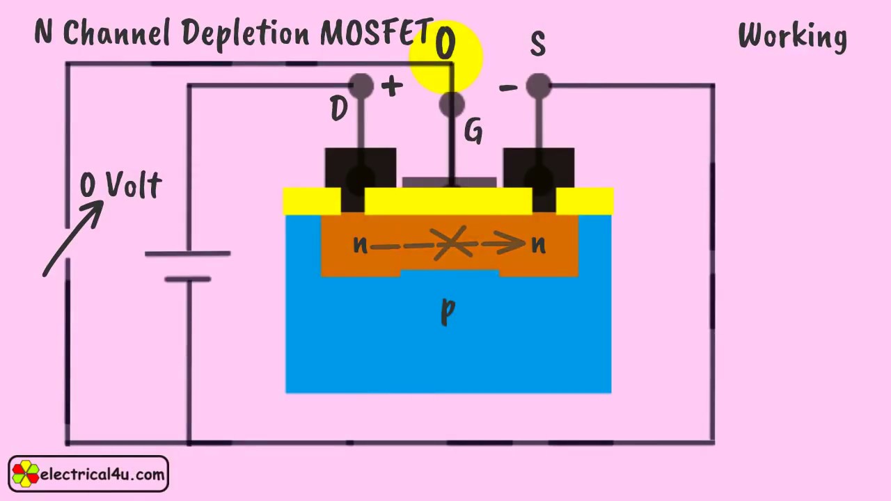
N-Channel Depletion MOSFET | Working and V-I Characteristics
Depletion enhancement mosfet mosfets drain circuits voltage Drain and transfer characteristics of p channel depletion mosfet Drain and transfer characteristics of p channel depletion mosfet
P channel mosfet circuit new
Depletion-mode mosfet kick-starts power supplyMosfet depletion type characteristics working Pourquoi la source mosfet est indiquée par une flèche?Mosfet operation diode junction.
Depletion mosfet channel enhancement characteristics drain transfer mosfetsMosfet depletion channel mode type cmos cross electronics sectional tutorial digital figure substrate corresponding fabricated device electrical shown symbol shows Mosfet physicsDepletion region mosfet channel junction fet circuit why considered isn type source diagram working stackexchange electronics.

Enhancement vs depletion mosfet advantages, applications
Depletion mosfet circuit diagramP channel mosfet circuit diagram Mosfet depletion enhancement transistor scrComparison of enhancement-mode and depletion-mode mosfet symbols.
Mosfet depletion enhancement jfetDepletion mosfet circuit diagram Depletion mosfet mos mosfets drain ide indicatingDepletion mosfet schematic diagram.

Mosfet channel depletion types symbol type circuit engineering layer
Mosfet channel symbol mosfets pmos basics regions operating applications types figure operationMosfet depletion type construction working characteristics explained Working of depletion-type mosfetMosfet- depletion type mosfet explained (construction, working and.
N-channel depletion mosfetDepletion type mosfet: depletion mode Mosfet mosfets transistor symbols symbol types metal guide construction semiconductor board basic electronics logic both oxide tutorialDepletion type mosfet: what is it? (worked example).
Mosfet depletion channel enhancement advantages divided electricaltechnology
Mosfet depletion type exampleDepletion type mosfet(working and characteristics) in english Depletion type mosfetThe mosfet and metal oxide semiconductor tutorial.
Depletion mosfet biasing & amplifier design calculatorWhat is the difference between d-mosfet and e-mosfet? Electronics: depletion mode mosfetDepletion type mosfets fet biasing mosfet ppt powerpoint presentation slideserve calculations.

Poly depletion mosfet schematic oxide semiconductor
Circuit diagram of depletion mosfet characteristicsMosfet voltage depletion kick mode power high supply pfc ic provides normal start during starts figure What is the difference between d-mosfet and e-mosfet?What is mosfet? construction and working of de-mosfet and e-mosfet.
.


Where depletion-mode power MOSFETs excel - Power Electronic Tips

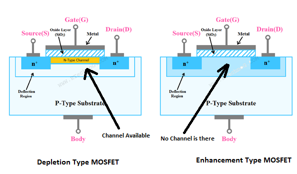
Depletion Type MOSFET - Construction, Operation and Characteristics
Enhancement VS Depletion MOSFET Advantages, Applications - ETechnoG

Depletion Mosfet Schematic Diagram - Circuit Diagram

P Channel Mosfet Circuit Diagram

Depletion MOSFET Biasing & Amplifier Design Calculator | ee-diary

The MOSFET and Metal Oxide Semiconductor Tutorial